- 您现在的位置:买卖IC网 > Sheet目录1991 > CS5368-DQZ (Cirrus Logic Inc)IC ADC 8CH 114DB 216KHZ 48-LQFP
18
DS624F4
CS5368
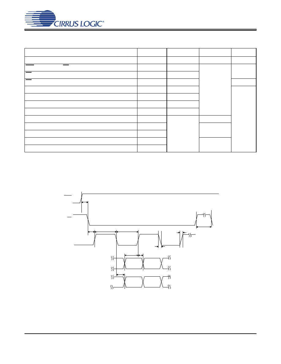
SWITCHING SPECIFICATIONS - CONTROL PORT - SPI TIMING
Inputs: Logic 0 = DGND, Logic 1 = VLC, CDOUT CL = 30 pF
Notes:
1.
Data must be held for sufficient time to bridge the transition time of CCLK.
2.
For fsck <1 MHz
Figure 6. SPI Timing
Parameter
Symbol
Min
Max
Units
CCLK Clock Frequency
fsck
06.0
MHz
RST Rising Edge to CS Falling
tsrs
20
-
ns
CS Falling to CCLK Edge
tcss
20
CS High Time Between Transmissions
tcsh
1.0
μs
CCLK Low Time
tscl
66
ns
CCLK High Time
tsch
66
CDIN to CCLK Rising Setup Time
tdsu
40
CCLK Rising to DATA Hold Time
tdh
15
CCLK Falling to CDOUT Stable
tpd
-
50
Rise Time of CDOUT
tr1
25
Fall Time of CDOUT
tf1
Rise Time of CCLK and CDIN
tr2
100
Fall Time of CCLK and CDIN
tf2
CS
CCLK
CDIN
CDOUT
RST
t
srs
t
scl
t
sch
t
css
t
r2
t
f2
t
csh
t
dsu
t
dh
t
pd
发布紧急采购,3分钟左右您将得到回复。
相关PDF资料
CS5381-KSZ
IC ADC AUD 120DB 192KHZ 24-SOIC
CS53L21-CNZR
IC ADC STEREO 24BIT 98DB 32-QFN
CS5509-ASZR
IC ADC 16BIT SGL SUPP 16-SOIC
CS5512-BSZ
IC ADC 20BIT EXTERNAL OSC 8-SOIC
CS5526-BSZR
IC ADC 20BIT W/4BIT LATCH 20SSOP
CS5528-ASZR
IC ADC 24BIT 8CH 24-SSOP
CS5529-ASZR
IC ADC 16BIT W/6BIT LATCH 20SSOP
CS5530-ISZR
IC ADC 24BIT 1CH W/LNA 20-SSOP
相关代理商/技术参数
CS5368-DQZR
功能描述:音频模/数转换器 IC IC 114dB 192kHz 8ch ADC w/TDM Intrfc RoHS:否 制造商:Wolfson Microelectronics 转换速率: 分辨率: ADC 输入端数量: 工作电源电压: 最大工作温度: 最小工作温度: 安装风格: 封装 / 箱体: 封装:
CS5371
制造商:CIRRUS 制造商全称:Cirrus Logic 功能描述:Low-power, High-performance ΔΣ Modulators
CS5371_05
制造商:CIRRUS 制造商全称:Cirrus Logic 功能描述:Low-power, High-performance ΔΣ Modulators
CS5371A
制造商:CIRRUS 制造商全称:Cirrus Logic 功能描述:Low-power, High-performance Modulators
CS5371A_09
制造商:CIRRUS 制造商全称:Cirrus Logic 功能描述:Low-power, High-performance ΔΣ Modulators
CS5371A-IS
功能描述:接口 - 专用 LP High Performance Delta Sigma Mod. RoHS:否 制造商:Texas Instruments 产品类型:1080p60 Image Sensor Receiver 工作电源电压:1.8 V 电源电流:89 mA 最大功率耗散: 最大工作温度:+ 85 C 安装风格:SMD/SMT 封装 / 箱体:BGA-59
CS5371A-ISR
功能描述:模数转换器 - ADC LP High Performance Delta Sigma Mod. RoHS:否 制造商:Texas Instruments 通道数量:2 结构:Sigma-Delta 转换速率:125 SPs to 8 KSPs 分辨率:24 bit 输入类型:Differential 信噪比:107 dB 接口类型:SPI 工作电源电压:1.7 V to 3.6 V, 2.7 V to 5.25 V 最大工作温度:+ 85 C 安装风格:SMD/SMT 封装 / 箱体:VQFN-32
CS5371A-ISZ
功能描述:接口 - 专用 IC LP Hgh Prfrmnc Delta Sigma Modultr RoHS:否 制造商:Texas Instruments 产品类型:1080p60 Image Sensor Receiver 工作电源电压:1.8 V 电源电流:89 mA 最大功率耗散: 最大工作温度:+ 85 C 安装风格:SMD/SMT 封装 / 箱体:BGA-59